If you already know or would rather not
know how these ccd's work or what the mod does then jump
straight to the next bit!.
The following is a quick overview of the ccds. Don't
treat it as an technical description but rather a model
which may help in piecing together information from
different sources.
Firstly the Sony CCD like most chips, comes in a standard
looking DIL package and is made of silicon. However its
worth making the distinction here between the common
digital devices and analogue ones such as the ccd.
Digital devices deal with on/off yes/no type signals
while the ccd's out put is a voltage which is proportion
to the light falling on the sensors.
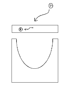 Figure 1 Figure 1 |
A schematic of a sensor is shown in
fig1 (the ccd contains an array of these sensors (659x494
in the case of the vesta's)). When a photon falls on the
sensor an electron is freed in the semiconductor. This is
able to travel for a while before becoming captured
again.
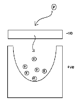 Figure 2 Figure 2 |
Figure 2 shows a voltage applied across
the surface of the ccd. Now when the electron is
liberated by the photon it is drawn into the 'well'
underneath. CCD's are characterised by the depth of these
wells (how may electrons the well can hold). The deeper
the wells the greater the dynamic range and the more
expensive the ccd. While the electron is in the well and
as long as the voltage across the chip is maintained the
electron is held. So we now have a system there the
collected electrons is proportional to the light hitting
the sensor. Next we need a way of reading this
information out.
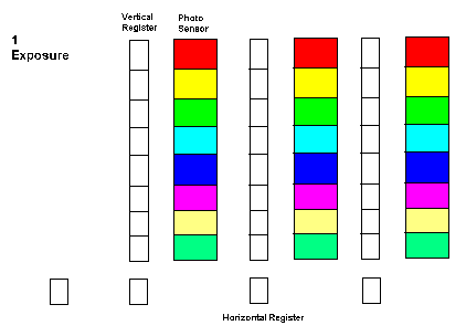 Figure 3 Figure 3 |
Also on the surface on the chip are a
series of vertical registers (one for each column of
sensors) and a horizontal register fig 3. Now we come to
the charge transfer pluses.
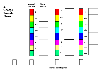 Figure 4 Figure 4 |
When these are applied the charge from
the sensors is moved in to the corresponding vertical
register. Fig 4.
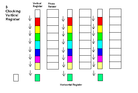 Figure 5 Figure 5 |
These registers are now clocked down
the chip using the vertical clock inputs to the chip.
Each clock cycle moves the pixels down by one, the bottom
pixel ending up in the horizontal register. (fig5).
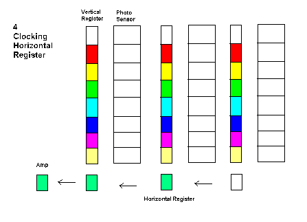 Figure 6 Figure 6 |
Finally the pixels are clocked along
this register though an on chip amplifier and out of the
ccd by the horizontal clocks. This signal then enters the
camera's a/d converted for conversion into a digital
signal.
With this much-simplified model we can get an idea of
what the mod is doing.
Firstly the mod disconnects the shutter pulse (pin 10 on
the vertical driver). To understand the shutter consider
the ccd running at 30 frames per second. The total time
the sensors are exposed would be 1/30th of a second.
However if there is no voltage applied across the chip
(fig1) then the freed electrons can't enter the well. If
the voltage is only applied or 1/2 the duration of each
frame (1/60th of a second) then the effective exposure
will be 1/60th of a second. What the shutter pulse is
doing is controlling the voltage across the chip. The
long exposure mod requires that the voltage is maintained
during the duration of the long exposure and so disables
the shutter control.
Next the chip read out. Using the standard divers the
slowest the rate the camera can be read out is 1/5th of a
second. However all the mod has to do to increase the
duration of the exposure is stop the accumulated charge
in the well from being moved into the vertical registers.
ie to block the charge transfer pluses. The most
convenient way of achieving this is at the vertical
driver chip. This chips takes the standard logic level
outputs of the cameras timing generator and converts the
signals the voltage levels required by the ccd. By
blocking this signal from pins 8 and 13 of this chip the
ccd no longer gets charge transfer pluses and the
electrons are allow to accumulate in the ccd's wells. Now
we have a long exposure but we still need a way of
re-enabling the charge transfer pluses to allow the image
to be read out. This is controlled by a signal from the
pc's printer port via the logic chip. When the printer
port signal is high then charge transfers are enabled and
vice versa. So all the mod is doing is disabling the
shutter and controlling the charge transfer pluses. This
means the vertical and horizontal clocks are left
running. This turns out to be a good thing. If these
clocks were stopped as well 'thermal noise' would build
up in these registers and lead to a degradation of the
image. Also the on chip amp is left powered. This is not
as good! On long exposure you will be able to see some
electro luminescents from this the top left hand part of
the image. This has to be removed together with 'hot'
pixels by dark frame subtraction.
|